
2 Inch GaN-on-Si Epi Wafer for HEMT and GaN Device Development
Product Description
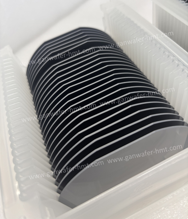
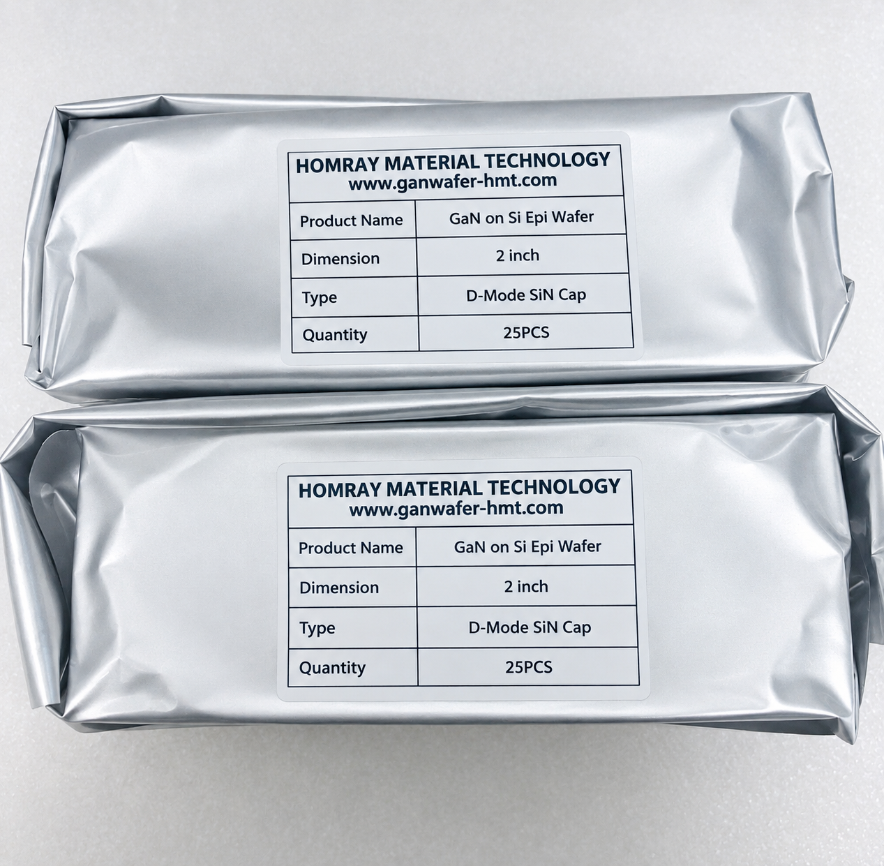
A 2 inch GaN-on-Si epi wafer provides a practical platform for GaN HEMT research, power device development, RF experiments, and epitaxial structure evaluation. HMT supplies GaN epitaxial wafers grown on Si(111) substrates using MOCVD, with customizable GaN, AlGaN, buffer, barrier, cap, and other epitaxial layers according to device requirements.
2 Inch GaN-on-Si Epi Wafer: A Compact Platform for GaN Device Development
A 2 inch GaN-on-Si epi wafer combines a silicon substrate with an engineered III-nitride epitaxial structure, providing a cost-effective material platform for laboratory development and pilot-scale semiconductor processing. Compared with larger production wafers, the 2 inch format is particularly useful for researchers who need to evaluate a new GaN epitaxial structure before moving to larger wafer diameters.
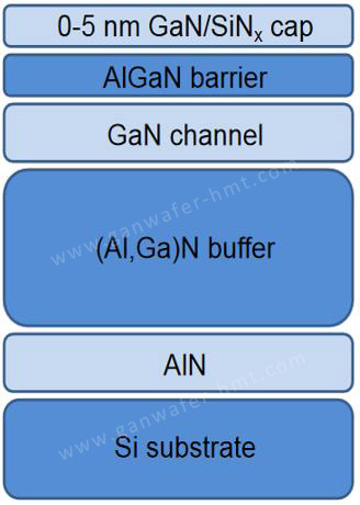
The substrate is typically silicon with a (111) orientation, while the epitaxial stack can be designed with an AlN nucleation layer, AlGaN transition or buffer layers, GaN channel layers, AlGaN barrier layers, and optional GaN or SiN cap layers. The final structure depends on the target application, device voltage, electrical characteristics, and fabrication process.
Why Choose a 2 Inch GaN-on-Si Epi Wafer?
The main advantage of a 2 inch GaN-on-Si epi wafer is development flexibility. A smaller wafer format allows universities, research laboratories, semiconductor startups, and device developers to test epitaxial structures without immediately committing to the material volume and processing requirements associated with 6 inch or 8 inch wafers.
GaN and silicon have different lattice constants and thermal-expansion behavior, making stress management an important part of GaN-on-Si epitaxy. A properly engineered buffer structure helps manage wafer stress, suppress defect propagation, and provide a more stable foundation for the GaN active layers.
For device development, the epitaxial structure can be tailored around the intended electrical architecture. Parameters such as GaN channel thickness, AlGaN barrier composition, barrier thickness, buffer structure, cap layer, and doping profile can be adjusted according to the customer's HEMT or power-device design.The material and device characteristics of GaN heterostructures have been extensively investigated in peer-reviewed semiconductor research.
Typical 2 Inch GaN-on-Si Epitaxial Structure
A representative GaN-on-Si structure can be arranged as follows:
2 Inch GaN-on-Si Epi Wafer Specifications
| Parameter | Typical / Available Specification |
|---|---|
| Wafer Diameter | 2 inch |
| Substrate | Silicon |
| Substrate Orientation | (111) |
| Growth Method | MOCVD |
| Epi Material | GaN / AlGaN/GaN |
| Buffer | AlN / AlGaN / GaN engineered structure |
| Application | HEMT, RF, power device R&D |
| Epi Thickness | Customized according to structure |
| Barrier Layer | AlGaN, customized |
| Cap Layer | GaN or SiN, optional |
| Wafer Structure | Customized |
MOCVD Growth for GaN-on-Si Epi Wafers
Metal-organic chemical vapor deposition (MOCVD) is widely used for III-nitride epitaxial growth because it provides precise control over layer composition, thickness, doping, and interface quality.
During GaN-on-Si growth, the nucleation and buffer regions are particularly important because the epitaxial stack must accommodate the material and thermal differences between GaN and silicon. Growth temperature, precursor flow, layer composition, stress compensation, and wafer temperature uniformity all influence the final wafer characteristics.
HMT can provide customized GaN-on-Si epitaxial structures for different research and device-development requirements rather than limiting customers to a single standard layer configuration.
GaN-on-Si for HEMT Development
AlGaN/GaN heterostructures are widely used for high-electron-mobility transistor development because polarization effects at the heterointerface can generate a high-density two-dimensional electron gas (2DEG).
In a typical AlGaN/GaN HEMT structure, the AlGaN barrier is positioned above the GaN channel. The resulting heterointerface provides the active channel required for high-frequency and high-power transistor architectures.
A 2 inch GaN-on-Si epi wafer is therefore useful for evaluating AlGaN barrier thickness, aluminum composition, GaN channel design, buffer structures, cap layers, and other parameters before scaling the process to larger wafers.For sensor and acoustic-wave research, HMT also supplies uid-GaN-on-Si epi wafers for piezoelectric and high-frequency device development.
2 Inch GaN-on-Si for Power Electronics
GaN-on-Si is particularly attractive for power electronics because silicon substrates offer large-scale manufacturing infrastructure and comparatively low material costs.
For power HEMT development, the epitaxial design must balance several parameters, including 2DEG characteristics, buffer leakage, breakdown behavior, wafer bow, defect density, and dynamic electrical performance. The 2 inch format can serve as a development platform for power-switching structures, allowing researchers to characterize a new epitaxial design before transferring the process to larger wafer sizes.
For customers developing enhancement-mode GaN power devices, HMT also provides GaN-on-Si epitaxial wafers designed for Power HEMT E-mode structures. For depletion-mode power switching development, customers can also evaluate HMT's GaN-on-Si D-HEMT epitaxial wafer platform.
GaN-on-Si for RF and Microwave Research
GaN HEMTs are also widely investigated for RF and microwave applications where high power density, high-frequency operation, and thermal stability are important.
For RF-oriented structures, the AlGaN barrier, GaN channel, buffer, and optional AlN spacer can be engineered to obtain the desired carrier concentration and transport characteristics. The exact structure should therefore be selected according to the intended operating frequency and device architecture rather than using one universal epitaxial recipe.
A 2 inch wafer is particularly suitable for university research, prototype fabrication, RF device experiments, and early-stage process development.
2 Inch GaN-on-Si vs. Larger GaN-on-Si Wafers
The primary difference between 2 inch and larger GaN-on-Si wafers is not the basic material system but the intended manufacturing stage.
A 2 inch wafer is generally more convenient for R&D, process verification, new structure evaluation, and small-volume prototyping. Larger 4 inch, 6 inch, and 8 inch wafers are more appropriate when the epitaxial structure has already been validated and the objective shifts toward higher wafer-level throughput and production scalability.
This makes 2 inch GaN-on-Si epi wafers a useful bridge between laboratory-scale material development and larger-scale semiconductor manufacturing.For applications where thermal management and RF performance are prioritized over substrate cost, GaN-on-SiC provides an alternative epitaxial platform.
Custom GaN-on-Si Epi Structures
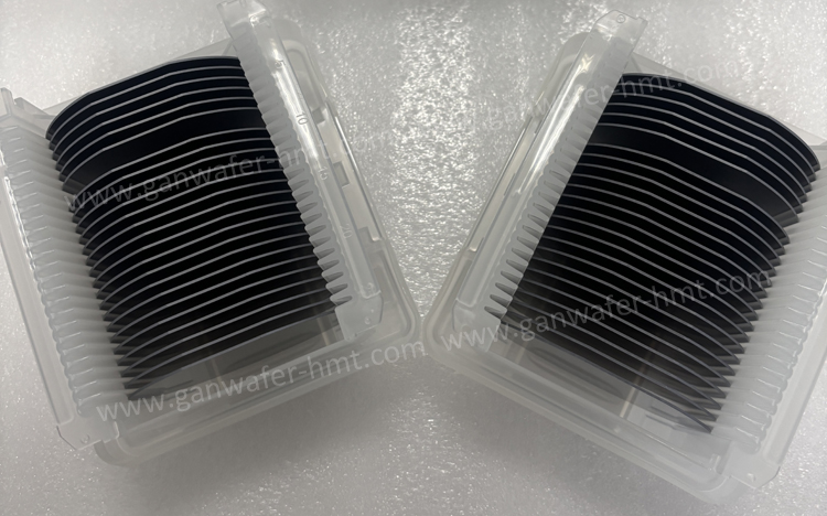
Different GaN devices require different epitaxial structures, so HMT supports customization of the epi stack according to customer specifications.
Potentially customizable parameters include:
- Si substrate diameter
- AlN nucleation layer
- AlGaN/GaN buffer structure
- GaN channel thickness
- AlGaN barrier thickness
- Aluminum composition
- AlN spacer layer
- GaN or SiN cap layer
Customers can provide their target layer structure or electrical requirements, and HMT can evaluate the appropriate GaN-on-Si epitaxial configuration.
Applications of 2 Inch GaN-on-Si Epi Wafers
GaN HEMT Research
2 inch GaN-on-Si wafers provide a convenient substrate platform for fabricating and evaluating AlGaN/GaN HEMTs and related heterostructure devices.
Power Device Development
The wafers can be used to investigate GaN power-switching structures, including enhancement-mode and depletion-mode device concepts.
RF and Microwave Devices
GaN-on-Si epitaxial structures can support research into RF transistors, microwave amplifiers, and high-frequency GaN devices.
Semiconductor Process Development
The 2 inch wafer format is suitable for developing etching, metallization, passivation, gate fabrication, and other semiconductor process steps before scaling to larger wafers.
University and Laboratory Research
Small-diameter GaN-on-Si wafers can reduce material consumption during early-stage experiments and make them practical for universities, research institutes, and semiconductor laboratories.

Frequently Asked Questions
What is a 2 inch GaN-on-Si epi wafer?
A 2 inch GaN-on-Si epi wafer is a silicon wafer with an engineered GaN-based epitaxial structure grown on its surface, typically using MOCVD. It can contain GaN, AlGaN, AlN, and optional cap or spacer layers depending on the target device.
What silicon substrate is used for GaN-on-Si epitaxy?
GaN-on-Si structures commonly use Si(111) substrates because this orientation is widely used for III-nitride epitaxial growth. The substrate thickness and resistivity can be selected according to the epitaxial and device requirements.
What is the typical structure of a GaN-on-Si HEMT wafer?
A representative structure consists of an Si substrate, AlN nucleation layer, AlGaN/GaN buffer, GaN channel, AlGaN barrier, and optional GaN or SiN cap layer. The exact stack depends on whether the target application is RF, power switching, or another GaN device architecture.
Related Products
 E-mail: kim@homray-material.com tina@homray-material.com
HMT Silicon Carbide (SiC) Substrate Website: www.sicsubstrate-hmt.com