
GaN epitaxy is a critical technology for manufacturing high-performance power, RF, and optoelectronic devices. As an experienced HMT GaN Epi Wafer Manufacturer, HMT provides GaN epitaxial wafer solutions based on Si, SiC, and sapphire substrates. By controlling epitaxial layer thickness, composition, doping, buffer structures, and surface quality, GaN epitaxy enables engineers to optimize device performance, reliability, and manufacturing compatibility. This article explains the fundamentals of epitaxy, major epitaxial growth technologies, GaN-on-SiC structures, and the role of GaN epi wafers in semiconductor manufacturing.
What Is GaN Epitaxy?
Epitaxy refers to the growth of a high-quality single-crystal layer with a specified structure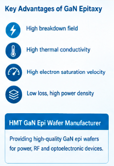 and properties on a carefully processed single-crystal substrate, typically after cutting, grinding, lapping, and polishing. The newly grown crystal layer follows the crystallographic orientation of the underlying substrate, essentially extending the original crystal structure outward.
The epitaxial layer can consist of the same material as the substrate or a different material. These structures are generally classified as homoepitaxy and heteroepitaxy, respectively. Because the newly formed single-crystal layer grows in accordance with the crystal orientation of the substrate, it is called an epitaxial layer, which typically has a thickness of several micrometers.
A substrate with an epitaxial layer is referred to as an epitaxial wafer, which can be understood as:
Epitaxial Wafer = Epitaxial Layer + Substrate
When the device is fabricated primarily within the epitaxial layer, the structure is commonly described as a conventional or forward epitaxial structure. When the device is fabricated on the substrate side and the epitaxial layer mainly serves as a supporting or functional layer, the structure may be referred to as a reverse epitaxial configuration.
For SiC and GaN semiconductor devices, one important approach to maximizing the inherent material advantages is to engineer high-quality epitaxial layers on single-crystal SiC substrates. The combination of a high-quality substrate and a precisely controlled epitaxial structure can provide the material platform required for advanced power, RF, and optoelectronic devices.
Why Are SiC and GaN Important Third-Generation Semiconductor Materials?
Third-generation semiconductor materials, represented by silicon carbide (SiC) and gallium nitride (GaN), offer significant advantages such as wide bandgaps, high electron saturation drift velocities, high thermal conductivity, and high critical breakdown electric fields. These properties make SiC and GaN ideal materials for developing electronic devices with high power density, high operating frequency, and low energy loss.
Why SiC Is Used for Power Devices?
SiC power devices offer advantages including high energy density, low power loss, and compact size, and have broad application prospects in new energy vehicles, photovoltaic systems, rail transportation, and data centers.
Why GaN Is Used for RF and Power Devices?
GaN RF devices provide high-frequency operation, high power density, wide bandwidth, low power consumption, and compact device dimensions, making them widely applicable to 5G communications, the Internet of Things (IoT), and military radar systems. In semiconductor manufacturing, growing high-quality epitaxial materials on suitable substrates is a key step in improving device performance and reliability and accelerating the adoption of third-generation semiconductor technologies in practical applications.
GaN Epi Wafer and Semiconductor Manufacturing
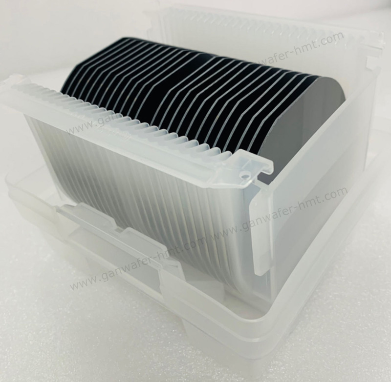
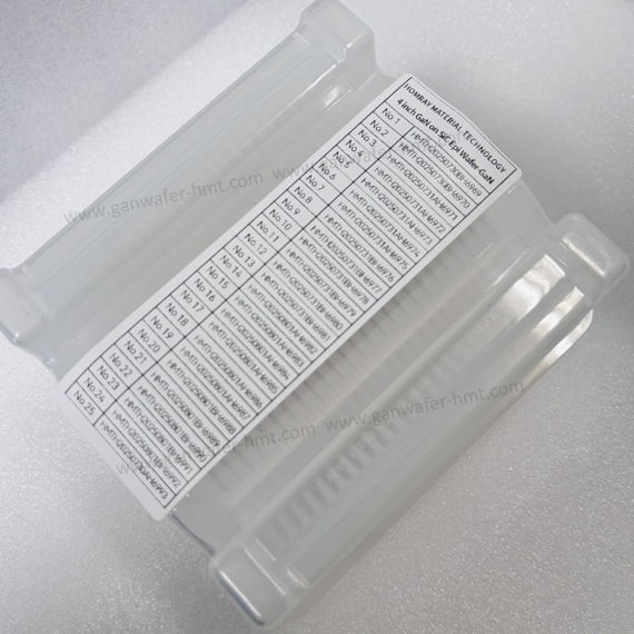
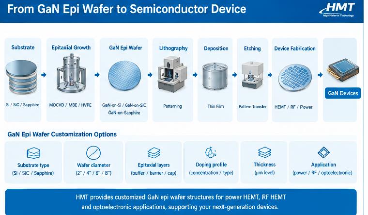
A GaN epi wafer consists of a semiconductor substrate and one or more epitaxially grown GaN-based layers. Depending on the target device, the substrate can be silicon, silicon carbide, or sapphire, while the epitaxial structure may contain GaN channels, AlGaN barriers, buffer layers, nucleation layers, p-GaN, or protective cap layers.
For power HEMTs, AlGaN/GaN heterostructures are commonly engineered to create a high-mobility two-dimensional electron gas (2DEG). For RF devices, GaN-on-SiC structures are attractive because the SiC substrate provides a thermally conductive platform for high-frequency and high-power operation. HMT manufactures GaN epi wafer structures for power HEMT, RF HEMT, and other specialized semiconductor applications, with substrate and epitaxial parameters available according to device requirements.
GaN Epi Wafer Substrate Options
GaN-on-Si Epi Wafer
For power HEMTs, GaN-on-Si epi wafers provide a scalable platform for AlGaN/GaN heterostructures on silicon substrates.HMT also provides pGaN-on-Si epi wafers for E-mode power HEMT structures.
GaN-on-SiC Epi Wafer
For RF applications, GaN-on-SiC epi wafers combine GaN heterostructures with the thermal properties of a SiC substrate.
GaN-on-Sapphire Epi Wafer
GaN-on-sapphire epi wafers remain an important platform for GaN-based optoelectronic devices.
Major GaN Epitaxial Growth Technologies
For compound semiconductors, epitaxy is a particularly important and specialized manufacturing process. Depending on the material system and target application, major epitaxial technologies include molecular beam epitaxy (MBE), metal-organic chemical vapor deposition (MOCVD), hydride vapor phase epitaxy (HVPE), and liquid-phase epitaxy (LPE).
MOCVD
Compared with other techniques, MOCVD generally provides a higher growth rate and is therefore well suited to large-scale industrial manufacturing.
MBE
MBE is known for its precise control over material composition and layer structure and can provide excellent material quality, although its growth rate is relatively slow. It is particularly useful for certain structures such as PHEMTs (pseudomorphic high-electron-mobility transistors) and some antimonide-based compound semiconductor materials.
HVPE
HVPE or hydride vapor phase epitaxy, is widely used for GaN and AlN epitaxial growth because of its relatively high growth rate. Many HVPE systems have historically been developed or customized for specific applications, although commercial equipment is also available. HVPE is particularly relevant to high-growth-rate GaN and thick GaN layer development, including GaN-on-sapphire structures and thick GaN templates.
LPE
GaN Epi Wafer Substrate Comparison
| Epi Structure | Typical Substrate | Main Applications | Key Consideration |
| GaN-on-Si | Si (111) | Power HEMT, RF | Large wafer size and manufacturing compatibility |
| GaN-on-SiC | 4H-SiC | RF HEMT, high-power RF | Thermal management and RF performance |
| GaN-on-Sapphire | Sapphire | LED, optoelectronics | Cost-effective optical applications |
| Free-standing GaN | GaN | Specialized GaN devices | Reduced heteroepitaxial mismatch |
Frequently Asked Questions About GaN Epitaxy
What is a GaN epi wafer?
A GaN epi wafer is a semiconductor wafer consisting of a substrate and one or more epitaxially grown GaN-based layers. Depending on the application, the substrate may be silicon, SiC, sapphire, or another suitable material.
What is the difference between GaN-on-Si and GaN-on-SiC?
GaN-on-Si uses a silicon substrate, while GaN-on-SiC uses a silicon carbide substrate. GaN-on-Si is widely developed for power and high-volume semiconductor applications, while GaN-on-SiC is commonly used for RF and high-power applications where substrate thermal properties are important.
Which epitaxial technology is commonly used for GaN epi wafers?
MOCVD is widely used for commercial GaN epitaxial wafer manufacturing because it provides controlled deposition of GaN-based heterostructures and is suitable for scalable production. MBE and HVPE are also important technologies for specific material structures and applications.
 E-mail: kim@homray-material.com tina@homray-material.com
HMT Silicon Carbide (SiC) Substrate Website: www.sicsubstrate-hmt.com