
Gallium nitride (GaN) devices depend heavily on the quality of their epitaxial layers, and substrate selection is one of the most important decisions in GaN manufacturing. The four major routes—GaN-on-Sapphire, GaN-on-Si, GaN-on-SiC and GaN-on-GaN—offer different combinations of cost, thermal performance, wafer size, crystal quality and device capability. The best substrate therefore depends on whether the target application is LED, power electronics, RF, microwave or vertical GaN devices.
What Is GaN Epitaxial Growth?
GaN epitaxial growth is the process of depositing a crystalline GaN or AlGaN/GaN layer onto a suitable substrate under controlled growth conditions. Unlike conventional silicon manufacturing, GaN devices commonly rely on heteroepitaxy because economical native GaN substrates are still more limited in wafer diameter and cost.
The epitaxial structure can include nucleation layers, buffer layers, GaN channels, AlGaN barriers and optional cap layers. These layers influence crystal quality, electrical characteristics, wafer stress, leakage, breakdown performance and ultimately device yield.
For commercial GaN epi wafers, MOCVD (metal-organic chemical vapor deposition) is one of the major technologies used to grow GaN-based semiconductor structures.
Why Does GaN Need a Foreign Substrate?
Silicon can serve as both the substrate and semiconductor material in conventional silicon integrated circuits. GaN manufacturing is different because large, economical native GaN wafers are less widely available than silicon or sapphire substrates.
Free-standing GaN substrates can provide an excellent homoepitaxial platform, but wafer diameter, crystal quality, growth rate and cost remain important considerations. As a result, heteroepitaxy remains central to commercial GaN manufacturing.
Three major foreign-substrate routes have become particularly important: GaN-on-Sapphire, GaN-on-Si and GaN-on-SiC.
GaN-on-Sapphire: A Mature Platform for Optoelectronics
Why Is GaN Grown on Sapphire?
Sapphire was one of the earliest commercially important substrates for GaN epitaxy and played a major role in the development of blue LEDs. Its relatively low cost, chemical stability and mature large-volume manufacturing infrastructure continue to make it important for optoelectronic applications.
However, sapphire has a substantial lattice mismatch with GaN and relatively low thermal conductivity. These characteristics require carefully engineered nucleation and buffer layers during epitaxial growth.
Advantages of GaN-on-Sapphire
- Mature manufacturing technology
- Relatively low substrate cost
- Excellent chemical stability
- Large wafer availability
- Extensive LED industry infrastructure
Limitations of GaN-on-Sapphire
The main limitations are the large lattice mismatch between GaN and sapphire, relatively high defect density and poor thermal conductivity compared with SiC.
Sapphire is also electrically insulating, which limits its suitability for device architectures requiring conventional lateral or vertical current conduction through the substrate.
Typical Applications
GaN-on-Sapphire is widely associated with:
- LED lighting
- Mini LED
- Display technologies
- Optoelectronic devices
- GaN device research and development
For these applications, manufacturing maturity and substrate economics can be more important than maximum thermal performance.
GaN-on-Si: A Cost-Driven Platform for GaN Power Devices
Why Is GaN-on-Si Important?
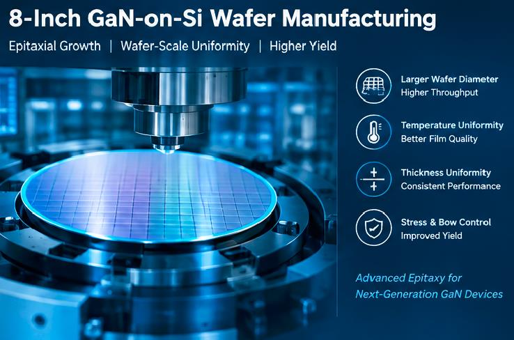
GaN-on-Si combines GaN device performance with the large wafer sizes and manufacturing infrastructure of silicon. Silicon substrates are available in established 6-inch and 8-inch formats, making this platform particularly attractive for cost-sensitive semiconductor manufacturing.
The fundamental advantage of GaN-on-Si is therefore not simply material compatibility—it is manufacturing economics and scalability.For research and prototype development, HMT also supplies 2 inch GaN-on-Si epi wafers with customized epitaxial structures for HEMT and GaN device development.
What Are the Main Challenges of GaN-on-Si?
GaN and silicon have different lattice constants and thermal-expansion behavior. GaN epitaxy is also performed at high temperatures, so cooling the wafer after growth can introduce substantial mechanical stress.
If this stress is not properly controlled, the wafer can experience bow, cracking or other structural problems. This makes buffer-layer design one of the most important technical aspects of GaN-on-Si epitaxy.
How Does Buffer Engineering Improve GaN-on-Si?
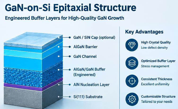
A typical GaN-on-Si structure can contain several transition layers between the silicon substrate and the active GaN layers.
A simplified structure may include:
- Si(111) substrate
- AlN nucleation layer
- AlGaN/GaN transition
- GaN channel
- AlGaN barrier
- Optional GaN or SiN cap layer
The exact architecture depends on wafer diameter, target voltage, device structure and MOCVD process.
Buffer engineering can influence wafer curvature, defect propagation, electrical isolation, leakage current and breakdown behavior. For this reason, the key challenge in GaN-on-Si is not simply growing GaN on silicon, but controlling stress, defects, bow and electrical performance simultaneously.For enhancement-mode power device development, HMT also supplies GaN-on-Si Power HEMT E-mode epi wafers with 2-inch to 8-inch substrate options.
Where Is GaN-on-Si Used?
GaN-on-Si is particularly important for:
- Power HEMTs
- Enhancement-mode GaN devices
- Depletion-mode GaN devices
- Power converters
- Fast chargers
- RF and microwave research
- GaN device development
- Semiconductor process development
IEEE research has also reviewed GaN-on-Si power technology in the context of device technology, applications, cost and commercialization.
GaN-on-SiC: A Performance-Oriented Platform for RF
Why Choose SiC as a GaN Substrate?
Silicon carbide provides a strong substrate platform for GaN RF devices because its thermal conductivity is substantially higher than that of sapphire and silicon. SiC also has a much smaller lattice mismatch with GaN than either sapphire or silicon.
These characteristics make GaN-on-SiC particularly attractive for high-power and high-frequency RF applications.
Advantages of GaN-on-SiC
- High thermal conductivity
- Lower lattice mismatch with GaN
- Strong thermal-management capability
- Suitable for high-power RF
- Suitable for microwave and mmWave devices
Limitations of GaN-on-SiC
The primary disadvantage is substrate cost. SiC wafers are significantly more expensive than silicon, and the supply chain is more concentrated.
Therefore, GaN-on-SiC is generally selected when thermal performance, RF capability and power density are more important than the lowest possible substrate cost.
Typical Applications
GaN-on-SiC is widely considered for:
- RF power amplifiers
- 5G infrastructure
- Radar
- Satellite communications
- Aerospace electronics
- Microwave systems
- High-power RF devices
Recent IEEE work has demonstrated GaN-on-Si HEMT technology for mmWave applications, illustrating that substrate selection continues to evolve according to the required combination of RF performance, efficiency and manufacturing economics.
GaN-on-GaN: The Homoepitaxial Route
What Is GaN-on-GaN?
GaN-on-GaN refers to epitaxial GaN grown on a native GaN substrate. Because the substrate and epitaxial layer have the same crystal material, the major lattice-mismatch problem associated with heteroepitaxy can be greatly reduced.
This provides an attractive route toward high-quality GaN structures with potentially lower defect densities.
What Limits GaN-on-GaN?
The main challenge is the availability and cost of native GaN substrates.
Free-standing GaN wafers remain more expensive and less widely available than silicon or sapphire substrates. Wafer diameter, crystal quality, substrate thickness and manufacturing economics are all important factors.
Why Is GaN-on-GaN Important for Vertical Devices?
GaN-on-GaN is particularly interesting for vertical GaN power devices, where current flows vertically through the semiconductor structure.
Compared with conventional lateral HEMT architectures, vertical GaN devices may offer a pathway toward high-voltage and high-current applications. However, commercial adoption depends heavily on improvements in native GaN wafer size, quality, availability and cost.
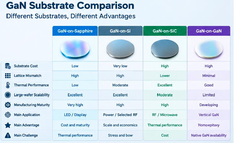
GaN-on-Sapphire vs GaN-on-Si vs GaN-on-SiC vs GaN-on-GaN
How Do You Choose the Right GaN Substrate?
The correct substrate depends on the target device and manufacturing priorities.
For LED and display applications, GaN-on-Sapphire remains attractive because of its mature supply chain, established manufacturing processes and low substrate cost.
For GaN power electronics, GaN-on-Si provides an attractive combination of large wafer availability, substrate economics and compatibility with scalable semiconductor manufacturing.
For high-frequency RF and microwave applications, GaN-on-SiC is often preferred when thermal management and power density are critical.
For advanced vertical GaN power devices, GaN-on-GaN provides a native homoepitaxial platform, although substrate cost and availability remain important barriers.
The most useful question is therefore not “Which GaN substrate is best?” but rather:
Which substrate provides the best balance of crystal quality, thermal performance, wafer size, manufacturing yield and total device cost for the intended application? For sensor and acoustic-wave research, HMT also provides uid-GaN-on-Si epi wafers for piezoelectric and high-frequency device development.
How HMT Supports Different GaN Epitaxial Platforms
Homray Material Technology provides GaN substrate and epitaxial wafer platforms covering GaN-on-Si, GaN-on-Sapphire and GaN-on-SiC, with different structures available for power, RF, research and other GaN device applications.
For customers evaluating GaN-on-Si structures, HMT offers epitaxial platforms covering 2-inch to 8-inch silicon substrates, including Power HEMT structures and customized epitaxial layer parameters.
For customers working on RF or high-frequency applications, GaN-on-SiC provides an alternative substrate platform where thermal management is a higher priority.
HMT also supplies GaN-on-Sapphire templates and free-standing GaN substrates for applications where sapphire or native GaN is more appropriate.
Conclusion
GaN epitaxial growth has developed into several distinct substrate routes rather than one universal manufacturing solution. GaN-on-Sapphire emphasizes maturity and cost, GaN-on-Si emphasizes manufacturing scale and economics, GaN-on-SiC emphasizes thermal and RF performance, while GaN-on-GaN provides a native homoepitaxial platform.
As GaN wafer diameters continue moving toward larger formats, the competitive advantage will increasingly depend on epitaxial uniformity, buffer engineering, wafer-bow control, defect management and manufacturing yield.
For device developers, selecting the right GaN substrate should therefore begin with the intended application, device architecture and manufacturing requirements rather than substrate material alone.
FAQ
What are the main GaN epitaxial growth routes?
The four major routes are GaN-on-Sapphire, GaN-on-Si, GaN-on-SiC and GaN-on-GaN. Each route offers a different balance of cost, thermal performance, wafer scalability and crystal quality.
Why is GaN-on-Si important for power electronics?
GaN-on-Si combines GaN device technology with the large wafer sizes and manufacturing infrastructure of silicon. This makes it particularly attractive for cost-sensitive power semiconductor applications.
 E-mail: kim@homray-material.com tina@homray-material.com
HMT Silicon Carbide (SiC) Substrate Website: www.sicsubstrate-hmt.com